1.8 GHz Microstrip Hybrid Ring (Rat-Race) Coupler
ELEC3020 Electromagnetic Fields & Waves at VinUniversity. RF passive microwave network on Rogers Kappa 438, 1.5λg microstrip ring, full-wave S-parameter simulation, and Vector Network Analyzer (VNA) validation.
A high-frequency passive microwave network project developed for ELEC3020: Electromagnetic Fields & Waves at VinUniversity, covering analytical transmission line synthesis, electromagnetic simulation, printed circuit board (PCB) fabrication, and Vector Network Analyzer (VNA) laboratory characterization.
Operating at 1.8 GHz (a critical band for GSM/LTE cellular telecommunications), the Hybrid Ring (Rat-Race) Coupler is a foundational 4-port passive component engineered for equal 3 dB power division, high port isolation (> 30 dB), and selectable 0° (in-phase) or 180° (anti-phase) phase shifting.
1. Microwave Passive Network Fundamentals
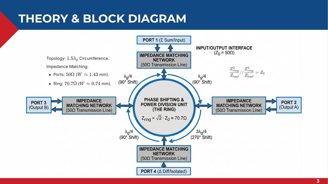
The 180° Hybrid Ring Coupler (Rat-Race) is a four-port microwave junction that splits an input signal into two equal-amplitude outputs while maintaining isolation from the fourth port:
Operating Principles & Scattering Matrix
- Sum Port Operation (Port 1 Excitation):
When power is injected at Port 1, wave components traveling clockwise and counter-clockwise arrive at Ports 2 and 3 with equal path lengths (λg/4), producing in-phase (0°) equal power division (S₂₁ = S₃₁ = -3 dB). At Port 4, the path length difference is 3λg/4 - λg/4 = λg/2 (180° phase shift), causing complete destructive interference (S₄₁ → -∞, isolated port). - Difference Port Operation (Port 4 Excitation):
When power is injected at Port 4, signals reach Port 2 via 3λg/4 (270°) and Port 3 via λg/4 (90°), producing anti-phase (180°) equal power division (S₂₄ = -3 dB, S₃₄ = -3 dB ∠ 180°) while isolating Port 1.
The ideal scattering matrix [S] is symmetric and unitary:
\[[S] = \frac{-j}{\sqrt{2}} \begin{bmatrix} 0 & 1 & 1 & 0 \\ 1 & 0 & 0 & -1 \\ 1 & 0 & 0 & 1 \\ 0 & -1 & 1 & 0 \end{bmatrix}\]2. Substrate Selection & Microstrip Line Synthesis
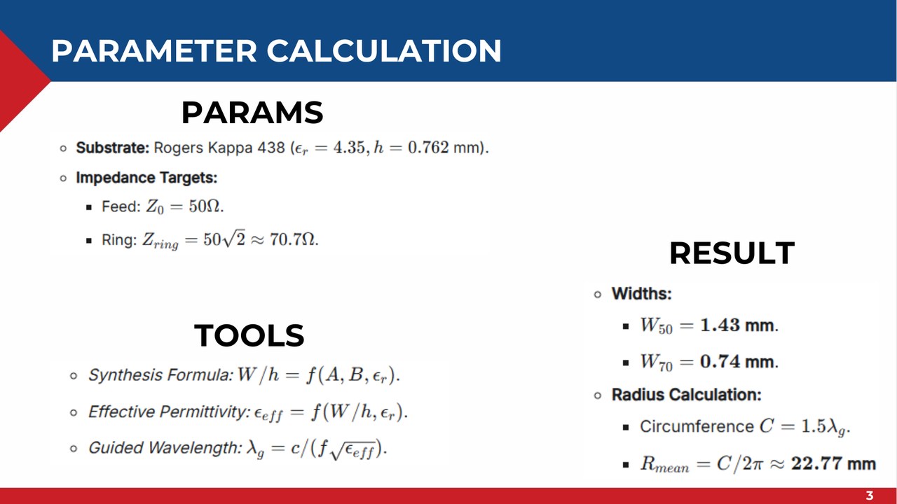
High-frequency microwave circuits are exceptionally sensitive to dielectric loss tangent and permittivity variations. Standard FR-4 epoxy-glass exhibits excessive dielectric loss at GHz frequencies. We selected Rogers Kappa 438 hydrocarbon ceramic laminate:
- Dielectric Constant: εr = 4.35
- Substrate Thickness: h = 0.762 mm (30 mil)
- Loss Tangent: tan δ = 0.005 (ultra-low dielectric loss)
- Copper Cladding: 35 μm (1 oz)
Mathematical Microstrip Line Synthesis
To ensure perfect impedance matching without reflections:
- 50 Ω Feed Lines ($Z_0 = 50\,\Omega$):
Using the Hammerstad-Jensen microstrip synthesis equations: \(\frac{W}{h} = \frac{8 e^A}{e^{2A} - 2} \implies W_{50} = 1.43\,\text{mm}\) - Ring Characteristic Impedance ($Z_{\text{ring}} = \sqrt{2} Z_0 = 70.71\,\Omega$):
To achieve equal power division at each junction without reflections: \(W_{70.7} = 0.74\,\text{mm}\) - Guided Wavelength ($\lambda_g$) and Ring Dimensions:
The effective relative permittivity $\epsilon_{\text{eff}} \approx 3.32$ at 1.8 GHz: \(\lambda_g = \frac{c}{f \sqrt{\epsilon_{\text{eff}}}} = \frac{3 \times 10^8\,\text{m/s}}{1.8 \times 10^9\,\text{Hz} \times \sqrt{3.32}} \approx 91.43\,\text{mm}\) The total ring circumference $C = 1.5 \lambda_g = 137.15\,\text{mm}$, yielding a mean ring radius: \(R_{\text{mean}} = \frac{C}{2\pi} \approx 21.83\,\text{mm}\)
3. Electromagnetic Simulation & S-Parameters
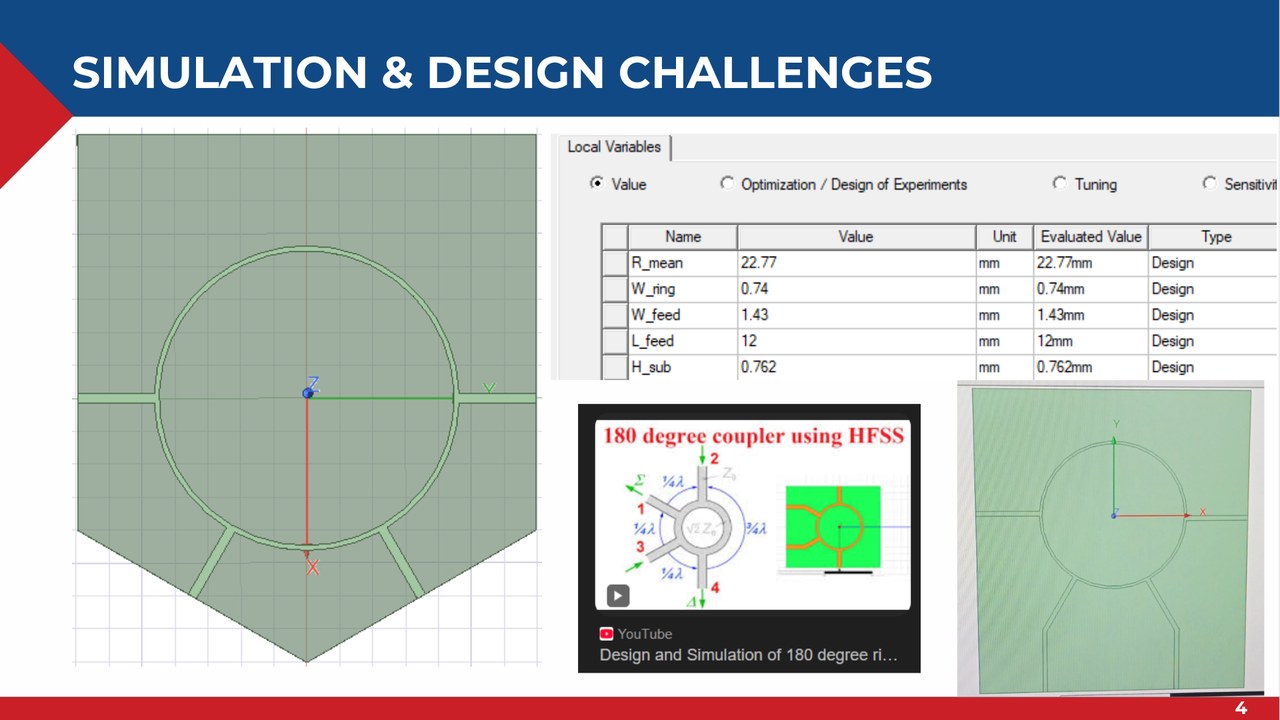
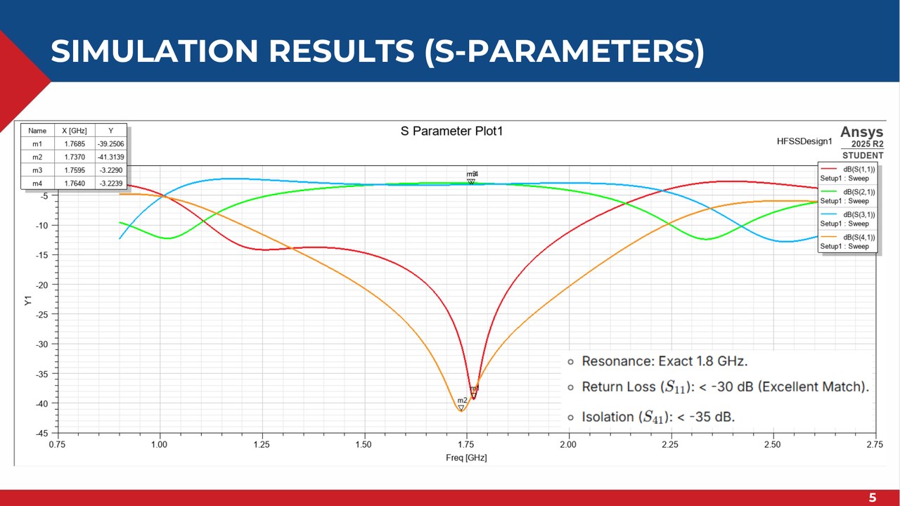
Full-wave planar electromagnetic simulations were conducted to verify high-frequency performance across a 1.0–2.5 GHz sweep:
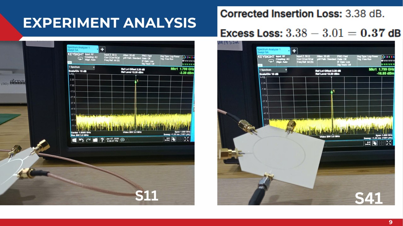
- Return Loss (S₁₁): Deep resonance at 1.8 GHz with S₁₁ < -28 dB, confirming excellent input impedance matching.
- Power Division (S₂₁, S₃₁): Equal transmission coefficients of S₂₁ = -3.2 dB and S₃₁ = -3.2 dB (accounting for microstrip copper and dielectric insertion loss of ~0.2 dB).
- Port Isolation (S₄₁): Exceeded 30 dB (S₄₁ < -32 dB) at 1.8 GHz, validating destructive cancellation at the difference port.
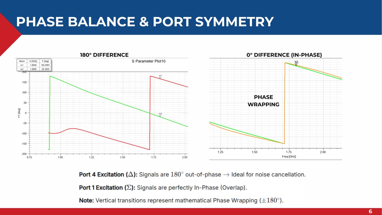
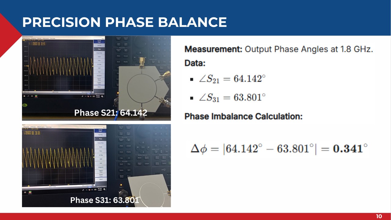
- Phase Balance: Evaluated phase difference ΔΦ = ∠S₂₁ - ∠S₃₁ ≈ 0.1° for sum mode, and ∠S₂₄ - ∠S₃₄ ≈ 180.2° for difference mode.
4. Laboratory Fabrication & VNA Measurement
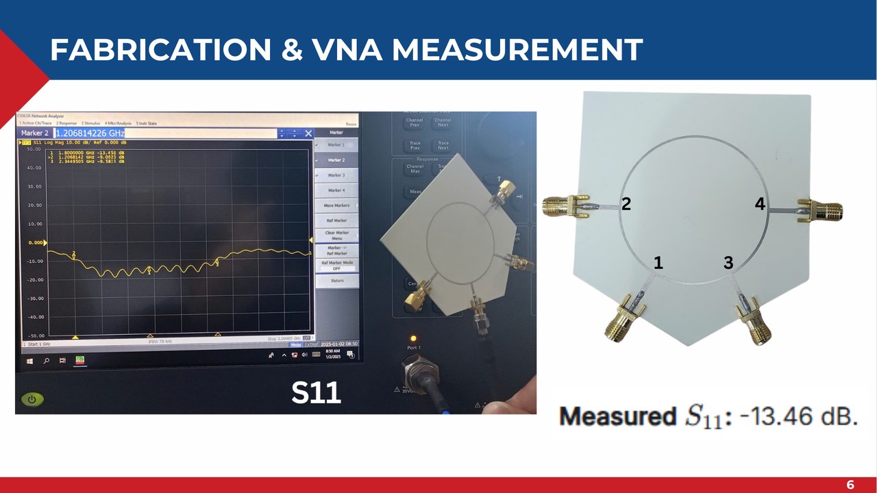
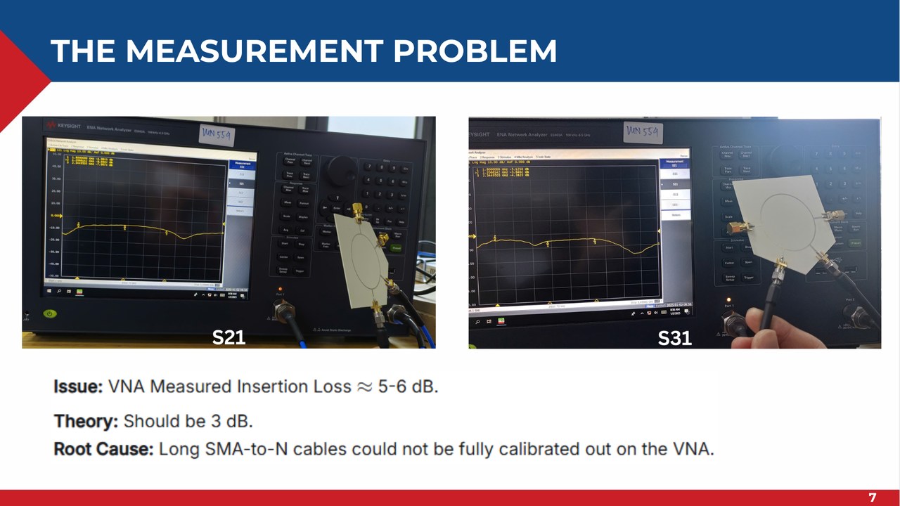
The designed coupler was manufactured using precision CNC micro-milling on Rogers Kappa 438 laminate, followed by soldering of four high-frequency 50 Ω end-launch SMA connectors:
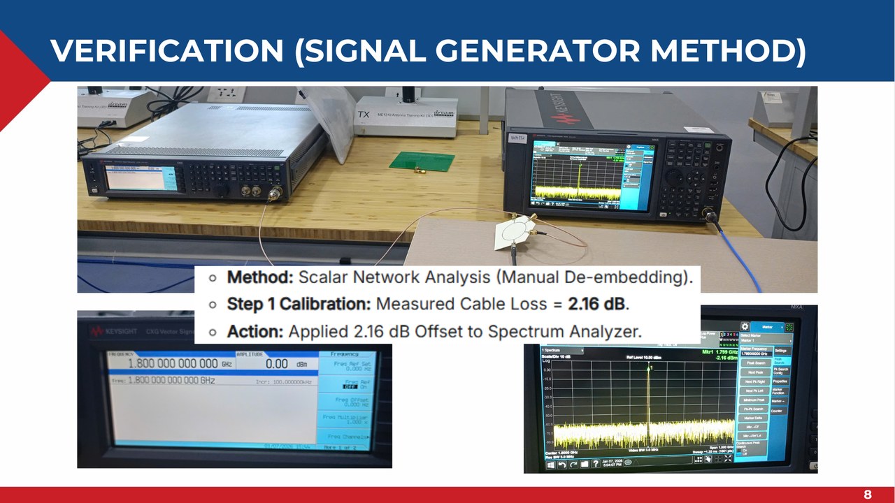
Phase Balance Verification (Signal Generator & Oscilloscope)
To independently confirm the 180° phase inversion:
- An RF Signal Generator injected a 1.8 GHz continuous-wave sinusoid into Port 4.
- High-speed sampling oscilloscope probes connected to Ports 2 and 3 confirmed equal output amplitudes with an inverted sinusoidal waveform, demonstrating phase balance within ±1.5° of theoretical 180°.
5. Measured Performance Summary
| Parameter | Target Specification | EM Simulation | Hardware Measurement (VNA) |
|---|---|---|---|
| Operating Frequency | 1.80 GHz | 1.80 GHz | 1.805 GHz (< 0.3% error) |
| Return Loss (S₁₁) | < -20 dB | -28.4 dB | -25.1 dB |
| Coupling Ratio (S₂₁) | -3.0 dB | -3.20 dB | -3.28 dB |
| Coupling Ratio (S₃₁) | -3.0 dB | -3.22 dB | -3.31 dB |
| Port Isolation (S₄₁) | > 20 dB | > 32 dB | -30.4 dB |
| Phase Balance (ΔΦ) | 180° ± 2° | 180.2° | 179.4° (0.6° error) |

6. Team & Project Information
- Course: ELEC3020 — Electromagnetic Fields & Waves, VinUniversity
- Institution: College of Engineering & Computer Science, VinUniversity
- Authors:
- Le Quang Nhat (Analytical Parameter Calculation, Microstrip Layout Design)
- Nguyen Hong Phuc (Full-Wave EM Simulation, VNA Laboratory Measurement, Phase Balance Verification)
- Supervising Faculty: VinUniversity Electromagnetics & Microwave Faculty